Thursday, November 22, 2012

UVM : Introduction

What is UVM

1)UVM is standardization in verification methodology by Accellera.
2) UVM is based on the best features in the existing methodologies OVM/VMM. But it is mostly derived from the OVM methodology and in fact it's backward compatible with the OVM. It has all the features of the proven OVM methodology
3) It is based on the System Verilog standard so it will compile on all the simulators which support the system Verilog standard.

The main advantages of UVM is :

1) Standardized verification methodology so no more confusion to choose a methodology to start a project.
2) No tool dependency. No more porting issues from one tool to other
3) Less confusion for the engineers. Easy to learn and maintain the skill set
4) Provides the flexibility and ways to connect the legacy VMM/OVM components
5) Backward compatible with OVM and provides the scripts to change OVM environment to UVM.
6) Remove the mess of having so many methodologies and provides a standard solution which compiles on all tools.


Universal Verification Methodology (From Wikipedia)


1. The Universal Verification Methodology (UVM) is a standardized methodology for verifying integrated circuit designs.

2. UVM is derived mainly from the OVM (Open Verification Methodology) which was, to a large part, based on the eRM (e Reuse Methodology) for the e Verification Language developed by Verisity Design in 2001.

3.The UVM class library brings much automation to the SystemVerilog language such as sequences and data automation features (packing, copy, compare) etc.,


History
1). lectronic design automation (EDA) industry — voted to establish the UVM and decided to base this new standard on the Open Verification Methodology (OVM-2.1.1)[1], a verification methodology developed jointly in 2007 by Cadence Design Systems and Mentor Graphics.

2). On February 21, 2011, Accellera approved the 1.0 version of UVM[2]. UVM 1.0 includes a Reference Guide, a Reference Implementation in the form of a SystemVerilog base class library, and a User Guide.[3].
The need of clocking blocks in testbench

The need of clocking blocks?
Clocking blocks have been introduced in SystemVerilog to address the problem of specifying the timing and synchronization requirements of a design in a testbench.
1) It is used to specify synchronization characteristics of the design
2) It Offers a clean way to drive and sample signals
3) It provides race-free operation if input skew > 0
4) It helps in testbench driving the signals at the right time
5) Features
    - Clock specification
    - Input skew,output skew
    - Cycle delay (##)
6) Can be declared inside interface,module or program

Example :
01.Module M1(ck, enin, din, enout, dout);
02.input         ck,enin;
03.input  [31:0] din    ;
04.output        enout  ;
05.output [31:0] dout   ;
06. 
07.clocking sd @(posedge ck);
08.input  #2ns ein,din    ;
09.output #3ns enout, dout;
10.endclocking:sd
11. 
12.reg [7:0] sab ;
13.initial begin
14.sab = sd.din[7:0];
15.end
16.endmodule:M1


#Skew : it is related to set up and hold time.

Input and Output Skew :
A skew number for an input denotes when that input is sampled before the clocking event (such as posedge or negedge) occurs. 
For an output, it is just the opposite - it denotes when an output is synchronized and sent after the clocking event.

clocking clock1 @(posedge clk1);
   input a1, a2;
   output b1;
endclocking
In this case, the default input skew is 1step and the default output skew is 0.

Overwriting default skews

Even if there is a default statement for skews in a clocking block, it can be overwritten later in the block. For example, the example below overwrites the default input skew for signal a1 (to 1step) and output b1 (to 5 ns), but the input skew for a2remains unchanged at 2 ns.
 
clocking clock1 @(posedge clk1);
   default input #2ns output #3ns;
   input #1step a1;
   input a2;
   output #5ns b1;
endclocking


VLSI Interview Questions : Part 1

What are the differences between SIMULATION and SYNTHESIS
i)Simulation <= verify your design.


Simulation is used to verify the functionality of the circuit.
a)Functional Simulation: a study of ckt's operation independent of timing parameters and gate delays.

b) Timing Simulation: study including estimated delays, verify setup, hold and other timing requirements of devices like flip-flops are met.
ii)Synthesis <= Check for your timing

Synthesis: One of the foremost in back-end steps whereby synthesizing is nothing but converting VHDL or VERILOG description to a set of primitives (equations as in CPLD) or components(as in FPGAs) to fit into the target technology.

Basically the synthesis tools convert the design description into equations or components


2. Differences between latches & flipflops?
There are 2 types of circuits:
1. Combinational
2. Sequential

Latches and flipflops both come under the category of "sequential circuits", whose output depends not only on the current inputs but also on previous inputs and outputs.
Difference: Latches are level-sensitive, whereas, FF are edge sensitive.
By edge sensitive, I mean O/p changes only when there is a clock transition.
( from 1 to 0 or from 0 to 1)

Example: In a flipflop, inputs have arrived on the input lines at time= 2 seconds. But, the output won't change immediately. At time = 3 seconds, clock transition takes place. After that, O/P will change.


Flip-flops are of 2 types:
1. Positive edge triggered
2. negative edge triggered

1) Flip-flops take twice the number of gates as latches
2) so automatically delay is more for flipflops
3) power consumption is also more


# Imp: latch does not have a clock signal, whereas a flip-flop always does.


3. What is slack?
The slack is the time delay difference from the expected delay(1/clock) to the actual delay in a particular path.
Slack may be +ve or -ve.


4. RTL and Behavioral
i) Register transfer language means there should be data flow between two registers and logic is in between them for end registers data should flow.

ii) Behavioral means how hardware behave determine the exact way it works we write using HDL syntax.For complex projects it is better mixed approach or more behavioral is used.


5. Equivalence between VHDL and C?
i)There is a concept of understanding in C there is structure. Based upon requirement structure provide facility to store the collection of different data types.

ii) In VHDL we have direct access to memory so instead of using a pointer in C (and member of structure) we can write interface to store data in memory and access it.

Difference between wire, reg and logic

1). Wire and Reg are present in the Verilog
2). System Verilog adds one more data type called logic.

Wire : 
1) Wire data type is used in the continuous assignments or ports list.
2) It is treated as a wire So it can not hold a value.
3) It can be driven and read.
4) Wires are used for connecting different modules.

Reg : 
1) Reg is a data storage element in System Verilog.
2) It's not an actual hardware register but it can store values.
3) Register retain their value until next assignment statement.

Logic : 
1) System Verilog added this additional datatype to make it easy to use the reg/wire datatype.
2) The main difference between logic datatype and reg/wire is that a logic can be driven by both continuous assignment or blocking/non-blocking assignment.

Source: asicguru.com (with little modification)

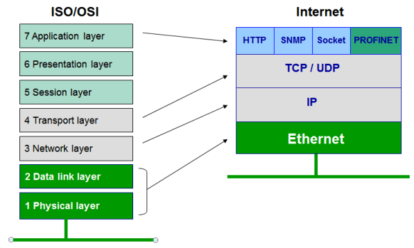
Ethernet and more

Ethernet is a protocol under IEEE 802.33 standard User Datagram Protocol (UDP) UDP is a connectionless transport protocol. I...